

Extracting Hidden IC Informations
Le Lab
We know how it feels to face a chip that refuses to reveal its secrets. For over 13 years, our independent laboratory has been dedicated to semiconductor depackaging, delayering, imaging and custom sample preparation.
our know-how
From Black Boxes to Actionable Insights
Le Lab is Texplained’s R&D-driven laboratory dedicated to extracting hidden information from integrated circuits (IC). We transform physical IC analysis into actionable technical knowledge for engineering, research, and strategic decision-making.
Advanced preparation & imaging
We perform depackaging, delayering, and high-resolution imaging (SEM and optical) to access internal IC layers and obtain the precise visual material required for reverse engineering and IC analysis.Controlled in-lab interaction
When needed, we conduct probing, wire bonding, and laser or electromagnetic fault injection (LFI & EMFI) to directly interact with semiconductor devices under controlled laboratory conditions.R&D-driven laboratory expertise
Our lab combines specialized equipment and proprietary tools such as ChipJuice to support rigorous hardware investigation workflows from physical access to deep technical validation.

1- Depackaging
Chip depackaging is the first essential step in semiconductor analysis and reverse engineering.
It consists in carefully removing the external package of an integrated circuit to access the silicon die without damaging its internal structures. This process combines mechanical and chemical techniques, selected according to the package type and materials.
Once the die is exposed, it can be inspected using optical and electron microscopy, electrically accessed, and prepared for further delayering and analysis.

2- Delayering
Chip delayering is a key step that consists in progressively removing the metal layers of an integrated circuit to reveal its internal structure. This process is performed in a controlled manner using a combination of mechanical, chemical etching, and plasma techniques. Each layer is exposed sequentially, allowing high resolution imaging of horizontal and vertical interconnections and transistors.
Throughout the process, optical and electron microscopy are used to monitor progress and ensure precision. Delayering enables accurate structural modification, layer-by-layer exposition, and reliable data extraction for further interpretation.
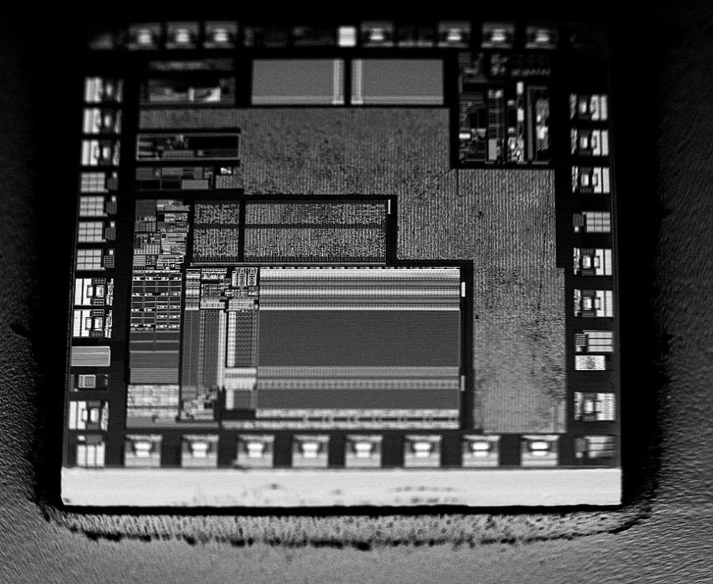
3- Imaging
Imaging is the bridge between physical access to the chip and meaningful analysis. By converting exposed structures into precise visual data, imaging allows patterns, layouts, and design physical implementations to be identified and digitally reconstructed. Optical and electron-based imaging techniques provide complementary views, from large-scale architecture down to fine structural details.
These images are then imported and processed using our specialized software ChipJuice, enabling reconstruction, in-depth analysis, and secret extraction.
High-quality imaging is essential for recovering and understanding chip functionality, conducting hardware analysis, and extracting the most hidden secrets.
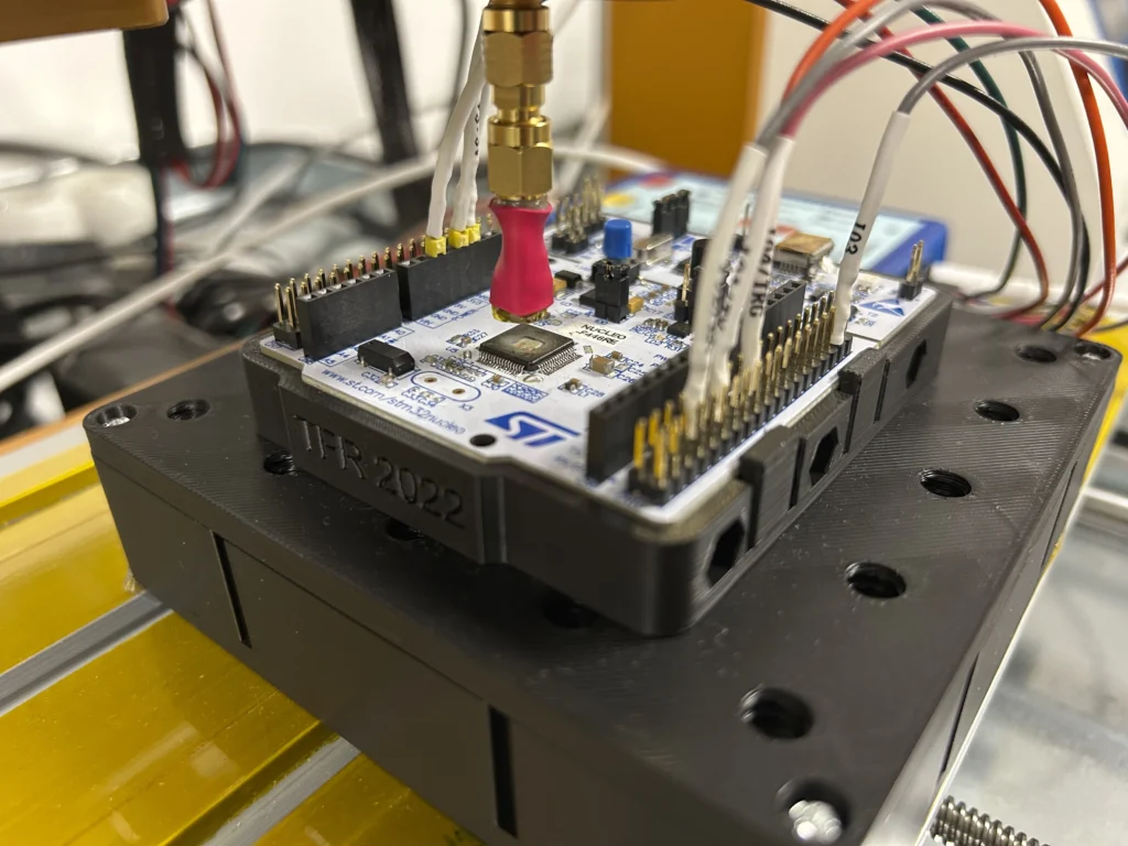
4- Advanced Extraction & Active Analysis
Our lab performs advanced operations designed to enable targeted data extraction and controlled interaction with integrated circuits.
A wire bonding station is used to recreate the connections to the depackaged chip, making it possible to use micro-probing to access internal nodes, allowing signal observation, direct manipulation, and retrieval of sensitive information.
Dedicated and custom LFI (Laser Fault Injection) and EMFI (Electro Magnetic Fault Injection) stations are used to inject localized and highly controlled perturbations, making it possible to trigger specific behaviours, bypass protections, or facilitate efficient extraction strategies built upon prior structural analysis.
These techniques transform structural understanding into practical exploitation capabilities & insights.
our equipment
The Tools Behind
Le Lab is equipped with advanced tools enabling precise access to integrated circuit layers, high-resolution imaging, and controlled interaction with semiconductor structures. Using specialized tools such as laser and electromagnetic fault injection stations, micro-probing systems, and dedicated test platforms, we conduct targeted hardware exploration and detailed chip-level investigations under strictly controlled conditions, supported by our patented ChipJuice software.
Chemical hood
Ventilated chemical hood enabling safe IC decapsulation, and chemical processing under controlled laboratory conditions.
Automated polisher
Precision automated polishing system for controlled material removal during IC cross-sectioning and layer-by-layer analysis.
Plasma etcher
Plasma etching equipment for selective material removal, dielectric thinning, and precise delayering of integrated circuits.
Probing station
Electrical probing station for direct IC testing and signal acquisition at wafer or die level.
SEM
Scanning Electron Microscope providing high-resolution imaging for the inspection and the reverse engineering of Integrated Circuits.
Wire bonding
Wire bonding station for creating reliable electrical connections between IC pads and PCBs.
Optical microscope
High-magnification optical microscope for surface inspection and preliminary IC structural analysis
Laser
Advanced laser-based station for high-resolution, localized fault induction in integrated circuits
EM station
Electromagnetic test bench for non-invasive side channel analysis and fault injection.