OUR LABORATORY
DEPACKAGING – DELAYERING – IMAGERY
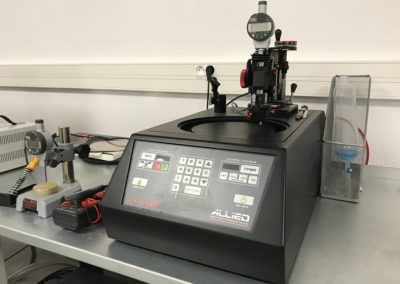
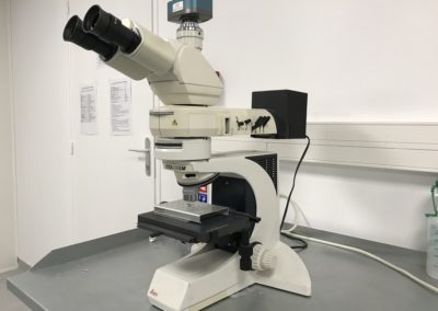
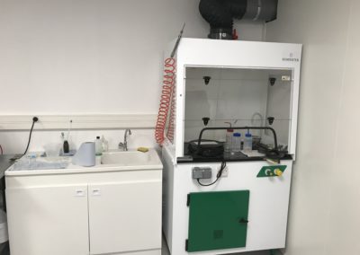
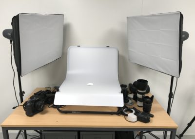
Our laboratory is an independent service laboratory specialising in the physical preparation, analysis and imaging of semiconductor devices and other electronic components. Services range in complexity from a simple mechanical cross-section of a Printed Circuit Board (PCB) to a full layer-by-layer deprocessing and imaging of an Integrated Circuit (IC). We use almost three decades of hands-on silicon experience to offer our clients a focused, efficient and comprehensive range of cost-effective solutions that meet, and regularly exceed their expectations.Our laboratory couples unique semiconductor hardware experience with a truly unique tool-set in our Sophia-Antipolis facility:
- Semiconductor Delayering and Imaging
- Semiconductor Cross Sectioning
- Semiconductor Package Cross Sectioning
- Chemical Processes
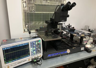
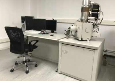
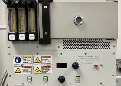
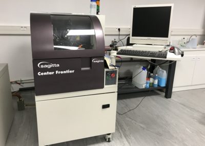
EQUIPMENTS DEDICATED TO REVERSE ENGINEERING
> 30 YEARS EXPERIENCE IN SAMPLE PREPARATION
CONDIFENTIALITY & QUALITY
.

